Schools
Senior secondary cohorts exploring semiconductors as a career or study pathway.
First exposure to how semiconductors works in practice. Site visits, expert briefings, and the scale of modern operations.
Typical group, 20–45 students

Industry
Foundries, fabless, and the geopolitics of silicon
Foundries, fabless design houses, and the packaging and test plants around them. Semiconductor tours reach the most strategically important supply chain on earth.
Duration
7–12 days typical
Group size
15–40 works best
Lead time
6–8 weeks for site access
Budget
From ₹1.5L per person (indicative)
Why this matters
01
Semiconductors sit under every other industry, and the geopolitics of who can make them has reshaped global trade. A cleanroom visit, even from behind the glass, communicates the extraordinary capital intensity and precision that a textbook can only gesture at.
02
Tibro concentrates its semiconductor routes on East Asia's fabrication heartlands and the design and equipment ecosystems around them, with hosted sessions that explain the full stack. Design, fabrication, assembly, test. And the strategic stakes.
03
Site visits in semiconductors require lead time, institutional relationships, and the right briefing. Tibro arranges hosted walkthroughs and expert sessions so the cohort leaves with operational detail, not a lobby tour.
Who it's for
Schools
First exposure to how semiconductors works in practice. Site visits, expert briefings, and the scale of modern operations.
Typical group, 20–45 students
Colleges & universities
Textbook concepts made concrete. Operations, supply chains, and strategy observed on the floor rather than in a case room.
Typical group, 15–35 participants
Companies & associations
Boardroom conversations opened by what the group has seen. Hosted access, peer networks, and transition roadmaps.
Typical group, 12–30 delegates
What you'll see
Wafer-fabrication cleanrooms (viewing)
Assembly, test and packaging plants
Chip-design and EDA houses
Semiconductor equipment makers
Materials and substrate suppliers
University microelectronics labs
Where we route cohorts
Five geographies we route semiconductors cohorts through most often. each with its own factory access, supplier networks, and learning focus.

Hosted semiconductors site visits and expert sessions across India. Factory access, institutional briefings, and sector context tailored to your cohort.

Hosted semiconductors site visits and expert sessions across Japan. Factory access, institutional briefings, and sector context tailored to your cohort.

Hosted semiconductors site visits and expert sessions across Germany. Factory access, institutional briefings, and sector context tailored to your cohort.
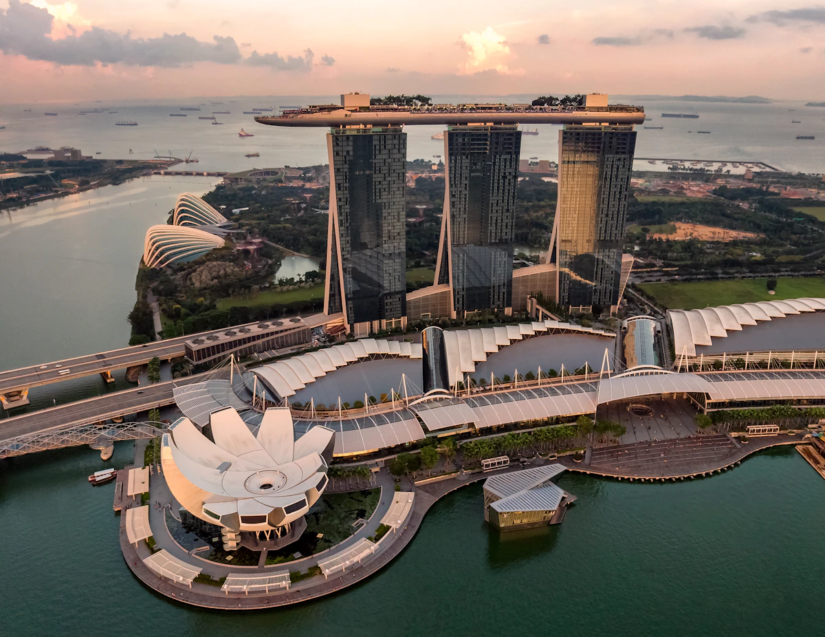
Hosted semiconductors site visits and expert sessions across Singapore. Factory access, institutional briefings, and sector context tailored to your cohort.

Hosted semiconductors site visits and expert sessions across USA. Factory access, institutional briefings, and sector context tailored to your cohort.
Practical notes
Duration
7–12 days typical
Group size
15–40 works best
Lead time
6–8 weeks for site access
Budget
From ₹1.5L per person (indicative)
Request a proposal
Headcount, dates, destination preference, and what the cohort should come home knowing. our knowledge-tours team responds within four business hours.
Related industries